cocotbext-ams
Tutorial: PWM DAC with SAR Controller
This tutorial walks through a complete mixed-signal co-simulation using cocotbext-ams. A hardware SAR (successive-approximation) controller binary-searches PWM duty cycles to digitize an unknown analog input voltage — the binary search runs entirely in Verilog RTL.
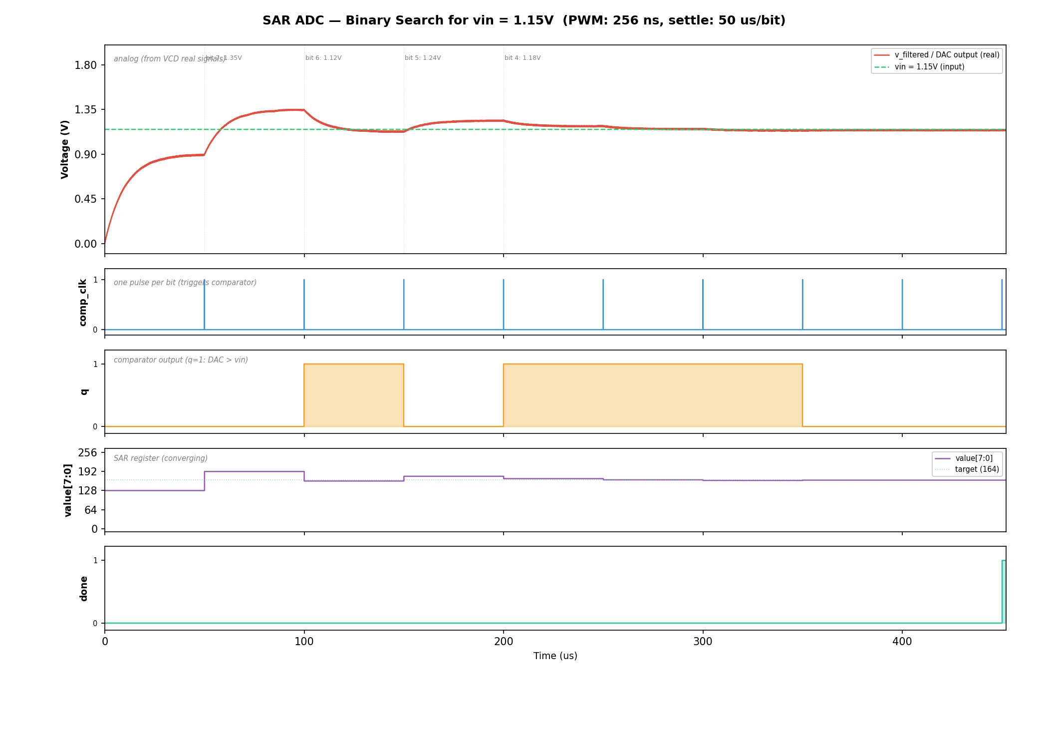
Example output: the SAR controller steps through values (visible as
changing PWM density), the RC-filtered DAC output steps toward vin, and
the comparator output q guides each bit decision. For vin = 1.15V, the
DAC output steps: 0.9V → 1.35V → 1.125V → … converging in 8 steps.
What you’ll learn
- Wiring a digital PWM to an analog RC filter in SPICE
- Using a sky130 standard-cell latch comparator for analog-to-digital conversion
- Building a SAR controller in Verilog that binary-searches duty cycles
- Configuring
DigitalPin,AnalogBlock, andMixedSignalBridge - Exporting mixed real/digital VCD waveforms for viewing
Prerequisites
- Python >= 3.10
- cocotb >= 2.0
- Icarus Verilog
- ngspice >= 45, built with
--with-ngshared(see README) - cocotbext-ams installed (
pip install cocotbext-ams) - sky130 PDK with
PDK_ROOTset:
export PDK_ROOT=/path/to/your/pdk    # e.g. /usr/share/pdk
# verify:
ls $PDK_ROOT/sky130A/libs.ref/sky130_fd_sc_hd/spice/sky130_fd_sc_hd.spice
Architecture
The adc module wraps all three components — the binary search runs
entirely in hardware:
                          adc module (adc.sv)
  ┌──────────────────────────────────────────────────────────┐
  │                                                          │
  │   SAR Controller          PWM Generator                  │
  │   (sar_controller.sv)     (pwm_gen.sv)                   │
  │                                                          │
  │   sar_clk ──> clk         clk ──> clk                    │
  │   comp_q <─── q ────┐     duty <────── value[7:0]       │
  │   value ─────────────┼──>  pwm_out ─────────┐            │
  │   done               │                      │            │
  │   comp_clk ────────┼──────────┐            │            │
  │                      │          v            v            │
  │                      │    Analog Block (SPICE)           │
  │                      │    (pwm_dac_stub.sv → ngspice)    │
  │                      │    ┌────────────────────────┐     │
  │                      └────┤ q          pwm_in <────┼─────┘
  │                           │ qb                     │     │
  │            comp_clk ───>│ clk                    │     │
  │              vin ────────>│ vin     RC Filter      │     │
  │              (analog)     │         10k + 1nF    │     │
  │                           │         Latch Comp     │     │
  │                           │         (sky130)       │     │
  │                           └────────────────────────┘     │
  └──────────────────────────────────────────────────────────┘
How the SAR works:
The SAR controller waits for the RC filter to settle, then pulses
comp_clk once to trigger the comparator. It reads q on the
next clock edge and decides the current bit:
q = 1→ DAC output > vin → value too high → clear bitq = 0→ DAC output ≤ vin → keep bit, try next
For vin = 1.15V with VDD = 1.8V, the DAC output steps through:
| Step | Bit | Value | DAC output | q | Decision |
|---|---|---|---|---|---|
| 0 | 7 | 128/256 | 0.90V | 0 | keep (DAC < vin) |
| 1 | 6 | 192/256 | 1.35V | 1 | clear (DAC > vin) |
| 2 | 5 | 160/256 | 1.13V | 0 | keep (DAC < vin) |
| 3 | 4 | 168/256 | 1.18V | 1 | clear (DAC > vin) |
| … | … | … | … | … | … |
Digital logic (Verilog): The SAR controller and PWM generator are
synthesizable RTL. The comparator output q is the only feedback from
the analog domain — it drives the entire binary search.
Analog (SPICE): The RC filter smooths the PWM into a DC voltage
(the DAC output), and the sky130 latch comparator compares it against
the analog input vin.
Bridge: cocotbext-ams connects them — ValueChange monitors
propagate pwm_out and comp_clk changes to SPICE instantly, and
threshold-crossing detection forces the comparator output q back
onto Verilog. The bridge uses a hierarchical block name
("dut.u_analog") to reach the SPICE stub inside the adc wrapper.
Files
| File | Purpose |
|---|---|
adc.sv |
Top-level ADC: SAR + PWM gen + analog comparator |
sar_controller.sv |
SAR binary search logic |
pwm_gen.sv |
PWM generator from duty register |
pwm_dac_stub.sv |
Verilog black-box stub for SPICE block |
rc_filter.sp |
RC low-pass filter subcircuit |
comp.sp |
Latch comparator subcircuit (sky130 cells) |
pwm_dac.sp |
Top-level SPICE wiring: filter → comparator |
tb_pwm_dac.sv |
Testbench instantiating the ADC |
test_pwm_dac.py |
cocotb test (drives clock, checks result) |
Makefile |
cocotb build/run |
Step 1: SPICE subcircuits
RC filter (rc_filter.sp)
.subckt rc_filter pwm_in vout vdd vss
r_filt pwm_in vout 10k
c_filt vout vss 1n
.ends rc_filter
A simple first-order low-pass with τ = 10kΩ × 1nF = 10μs.
Latch comparator (comp.sp)
.subckt comp vinp vinm clk q qb vdd vss
* Cross-coupled NOR3 + NAND3 pairs using sky130 standard cells
* Latches on rising edge of clk
* Outputs q/qb are rail-to-rail digital
...
.ends comp
Uses sky130_fd_sc_hd__nor3_1, sky130_fd_sc_hd__nand3_1, and
sky130_fd_sc_hd__inv_1. The outputs are standard-cell logic levels,
so digitizing them with a threshold makes perfect sense.
Top-level (pwm_dac.sp)
.subckt pwm_dac pwm_in clk vin q qb vdd vss
Xrc   pwm_in v_filtered vdd vss rc_filter
Xcomp v_filtered vin clk q qb vdd vss comp
.ends pwm_dac
The comparator’s vinp receives the DAC output (RC-filtered PWM),
and vinm receives the analog input vin being digitized.
Step 2: Digital RTL
PWM generator (pwm_gen.sv)
module pwm_gen #(parameter N_BITS = 8)(
    input  wire              clk,
    input  wire              reset_n,
    input  wire [N_BITS-1:0] duty,
    output reg               pwm_out
);
    reg [N_BITS-1:0] counter;

    always @(posedge clk or negedge reset_n) begin
        if (!reset_n) begin
            counter <= 0;
            pwm_out <= 0;
        end else begin
            counter <= counter + 1;
            pwm_out <= (counter < duty);
        end
    end
endmodule
With N_BITS=8 and a 1 GHz clock, one PWM period = 256 × 1ns = 256 ns. The value register directly controls the DAC output voltage: V_filtered ≈ (value / 256) × VDD.
SAR controller (sar_controller.sv)
module sar_controller #(
    parameter N_BITS        = 8,
    parameter SETTLE_CYCLES = 500  // sar_clk cycles to wait per bit
)(
    input  wire              clk,        // SAR clock
    input  wire              reset_n,
    input  wire              comp_q,     // 1 = DAC output > vin
    output reg [N_BITS-1:0]  value,      // converging digital value
    output reg               done,
    output reg               comp_clk  // pulses once per bit
);
The SAR controller works MSB-first. For each bit:
- On reset, sets
value = 10000000(MSB tentatively set) - Waits
SETTLE_CYCLESfor RC filter to converge - Pulses
comp_clkto trigger the comparator - Reads
comp_qon the next clock edge- If
comp_q = 1(DAC > vin): value too high → clear the bit - If
comp_q = 0(DAC ≤ vin): keep the bit set
- If
- Sets the next bit tentatively and repeats from step 2
- After 8 bits, asserts
donewith the final value
With a 10 MHz SAR clock and SETTLE_CYCLES = 500, each bit takes
50 μs = 5τ to settle, ensuring the DAC output reaches a stable value.
ADC wrapper (adc.sv)
module adc #(
    parameter N_BITS        = 8,
    parameter SAR_DIV       = 100,  // clk divider for SAR clock
    parameter SETTLE_CYCLES = 50
)(
    input  wire              clk,        // fast clock (drives everything)
    input  wire              reset_n,
    input  wire              vin,        // analog input to measure
    output wire [N_BITS-1:0] value,
    output wire              done
);
    wire pwm_out, q, qb, comp_clk;

    // SAR clock: clk / SAR_DIV
    // comp_clk: generated by SAR controller (once per bit)

    pwm_dac u_analog (                        // SPICE stub
        .pwm_in(pwm_out), .clk(comp_clk),
        .vin(vin), .q(q), .qb(qb)
    );
    pwm_gen #(.N_BITS(N_BITS)) u_pwm_gen (    // PWM generator
        .clk(clk), .reset_n(reset_n),
        .duty(value), .pwm_out(pwm_out)
    );
    sar_controller #(                          // SAR logic with settling
        .N_BITS(N_BITS), .SETTLE_CYCLES(SETTLE_CYCLES)
    ) u_sar (
        .clk(sar_clk), .reset_n(reset_n),
        .comp_q(q), .value(value), .done(done),
        .comp_clk(comp_clk)
    );
endmodule
The adc module encapsulates the complete system. A single clk
input is divided down internally to produce the SAR clock. The
comparator is latched by comp_clk from the SAR controller —
only once per bit, at the end of each settling period. The SPICE
stub (u_analog) is inside the wrapper, so the bridge uses a
hierarchical block name "dut.u_analog" to reach it.
Step 3: Verilog testbench
module tb_pwm_dac;
    reg clk, reset_n;
    wire [7:0] value;
    wire done, vin;

    adc #(.N_BITS(8), .SAR_DIV(100), .SETTLE_CYCLES(500)) dut (
        .clk(clk), .reset_n(reset_n),
        .vin(vin), .value(value), .done(done)
    );
endmodule
Single clock domain:
clk(1 GHz): Fast clock for the PWM counter. With 8 bits, PWM period = 256 ns ≪ RC τ = 1 μs, so the filter output is smooth. Divided by SAR_DIV=100 internally → 10 MHz SAR clock.SETTLE_CYCLES = 500→ 50 μs (= 5τ) settling per bit. Comparator latched once per bit by the SAR controller.
Step 4: cocotb test
The Python test is minimal — the binary search runs in hardware:
# The analog block is inside the adc wrapper — use hierarchical name
pwm_dac = AnalogBlock(
    name="dut.u_analog",   # path to SPICE stub inside adc module
    spice_file="pwm_dac.sp",
    subcircuit="pwm_dac",
    digital_pins={...},
    analog_inputs={"vin": 1.15},    # analog input to digitize
    ...
)

bridge = MixedSignalBridge(dut, [pwm_dac], max_sync_interval_ns=50)
await bridge.start(duration_ns=sim_duration, analog_vcd="pwm_dac_analog.vcd",
                   vcd_nodes=["v_filtered"])

# Start single fast clock (SAR clock + comp_clk derived internally)
cocotb.start_soon(Clock(dut.clk, 1, "ns").start())  # 1 GHz

# Release reset and let the SAR run
dut.reset_n.value = 1
# ... wait for done ...
await RisingEdge(dut.done)

result = int(dut.dut.u_sar.value.value)
The test watches the comparator output q at each SAR step, showing
the binary result being built up bit by bit:
SAR ADC: digitizing vin=1.15V  (expect value≈163/256)
  bit[7]: q=0 → 1  |  1.......  v_filtered=0.900V
  bit[6]: q=1 → 0  |  10......  v_filtered=1.350V
  bit[5]: q=0 → 1  |  101.....  v_filtered=1.125V
  bit[4]: q=1 → 0  |  1010....  v_filtered=1.181V
  ...
Result: 10100011 (0xA3) = 163/256 → 1.147V  (vin=1.150V)
Step 5: Run
cd docs/tutorial
export PDK_ROOT=/path/to/your/pdk
make
Step 6: View waveforms
Two VCD files are produced:
| File | Contents |
|---|---|
tb_pwm_dac.vcd |
Digital signals: value[7:0], done, pwm_out, comp_clk, clock |
pwm_dac_analog.vcd |
Analog voltages ($var real) + digitized outputs ($var wire) |
Load both in your viewer:
surfer tb_pwm_dac.vcd pwm_dac_analog.vcd
What you’ll see:
value[7:0](digital): the SAR register converging bit by bitpwm_out(digital): PWM density changing as value updatesv_filtered(real): the DAC output stepping toward vinvin(real): the analog input being digitized (constant 1.15V)q(digital): comparator output guiding each SAR decisioncomp_clk(digital): single pulse per bit, triggers comparatordone(digital): asserted when conversion completes
How it works under the hood
-
SAR sets a bit in the value register → PWM generator immediately changes its output density →
ValueChangemonitor propagates the newpwm_outto SPICE instantly. -
RC filter integrates the new PWM at full analog resolution. The VCD writer records the smooth
v_filteredtrace stepping up or down as each bit is tested. -
SAR pulses
comp_clkonce after settling. The comparator latches the current DAC output vs. vin. Whenqcrosses the digital threshold, event-driven sync forces the value onto Verilog. -
SAR reads
qon the next clock edge and decides to keep or clear the bit. -
After 8 steps,
donegoes high andvalueholds the final N-bit digital result representingvin.
Next steps
- Change N_BITS to 10 for higher resolution (needs longer simulation)
- Add
hysteresis=0.1to the outputDigitalPinto prevent glitching - Try different RC values and observe settling behavior
- Look at the SAR ADC example for a full data converter
- See the API reference for all options